Applications:
Semiconductors
AFM-in-SEM focus on semiconductor manufacturing, failure analysis, research and development.
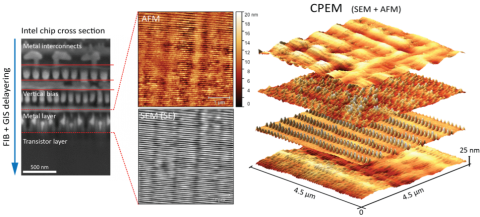
Integrated Circuit Pickling
Due to miniaturization, failure analysis of advanced integrated circuits is only possible by removing locally focused ion beam (FIB) layers. It is necessary to evaluate the flatness and roughness of pickled surfaces.
Benefits of LiteScope:
- Precise identification of a particular layer, excellent planarity of milled FIB structures with minimal damage to the sample. 3D Reconstruction: in situ evaluation of the topography and roughness of the milled structure.
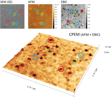
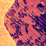
Images of thread dislocations in GaN/AlN/Si films
Gallium nitride (GaN) is a very promising material for electronic and optoelectronic applications; however, a variety of dislocations can occur at the interface of different materials, leading to poor quality films.
Benefits of LiteScope:
- Various defects can be located and characterized by the CPEM view alone, combining AFM, SEM, and EBIC (Electron Beam Current). CPEM allows direct comparison between surface topography, electrical activity, and surface chemistry of the sample.
Published courtesy of: Roman Gröger, IPM CAS, Czech Republic
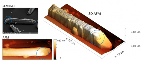
Gallium arsenide (GaAs) nanowires
Semiconductor nanowires are becoming increasingly important due to their novel electronic, photonic, thermal, electrochemical, and mechanical properties. GaAs nanowires have been explored for a wide variety of possible devices, including transistors, photodetectors, LEDs, solar cells, and nanolaser devices. The optimization of the synthesis of GaAs nanowires is crucial to obtain the expected characterizations. Correlative AFM-in-SEM microscopy facilitates efficient quality control and complex analysis of nanowires.
Benefits of LiteScope:
- Fast and precise localization of a single nanowire. Complex characterization of structures and composition of a single nanowire using SEM material contrast and 3D AFM profiles.
Published courtesy of: David Fuster, Andrés Raya, Álvaro San Paulo and María Ujue González, CNM, CSIC Madrid, Spain
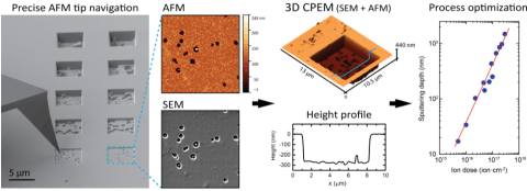
Surface modification of cadmium telluride
Cadmium telluride (CdTe) is a semiconductor with a wide range of applications ranging from X-ray or gamma-ray detectors to solar cells. Due to the heterogeneity of the CdTe compound, the planarity of the focused ion beam (FIB)-etched structures is uneven and requires optimization of the FIB milling process.
Benefits of LiteScope:
- Surface modification using FIB/GIS techniques can be performed directly on a tilted LiteScope within SEM, which is crucial for sensitive samples prone to oxidation.Immediate evaluation of the modified surface profile and process quality control.Process optimization FIB milling by sputtering rate and roughness estimation.
Published courtesy of: Ondrej Sik and Martin Konecny, CEITEC BUT, Czechia
Material science
More information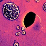
Nanostructures