


SEM / STEM
Scanning transmission electron microscopy (STEM) combines the principles of transmission electron microscopy and scanning electron microscopy and can be performed on either type of instrument. Like TEM, STEM requires very thin samples and looks primarily at beam electrons transmitted by the sample. One of its principal advantages over TEM is in enabling the use of other of signals that cannot be spatially correlated in TEM, including secondary electrons, scattered beam electrons, characteristic X-rays, and electron energy loss.
In the SEM / STEM we work at low acceleration voltages but we can achieve subnanometric resolutions (0.6 nm), which makes it a very efficient alternative from the economic point of view to a TEM / STEM.
- Observation of multiple samples without braking the chamber vacuum.
- Simultaneous acquisition of bright field (BF), dark field (DF) and high angle dark field (HADF) signals which provide valuable information such as Bragg-diffraction orientation contrast and material contrast.
- Lifting up and down of the sample relative to the detector in order to reach the best imaging conditions.
- Tilting of the sample independently of the detector
- Improved geometry of the sample holders for EDX analysis
Excellent platform suitable for SEM/STEM metrology at sub-nanometer scale
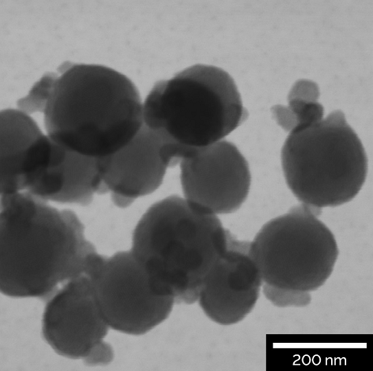
Morphology of nanoparticles used in drug delivery
research visualized by R-STEM detector at 30 keV