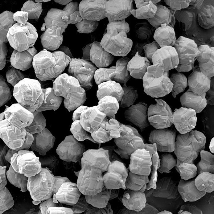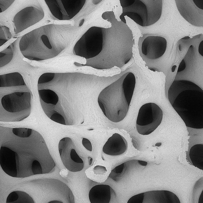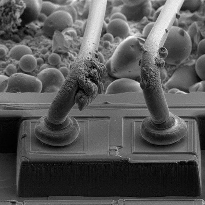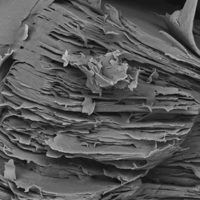
Applications
The constant progress of modern science and the rapid development of technology require more and more advanced technologies that can satisfy the growing demand for high-resolution imaging, sample modification and analysis. This is the case of the semiconductor industry where the physical dimensions of microelectronic devices continue to shrink making failure analysis an extremely challenging task. At the same time, materials science is now one of the most active and exciting fields of science that requires sophisticated analytical tools in order to characterise and understand new materials that show striking physical properties. Recent investigations of cell morphology and biotechnology heavily rely on state-of-the-art techniques for microanalysis.
TESCAN world-class technology delivers complete solutions for researchers in all branches of science. No matter what is the type and size of the sample, and what questions are being asked, there is always a dedicated solution available to solve all required tasks. Due to high versatility and customisable design of all TESCAN systems, it is very easy to design and manufacture dedicated instruments suited exactly to the customer’s needs.