Semiconductors & Microelectronics
Scanning electron microscopy (SEM), in combination with focused ion beams (FIB), is an ideal technique for keeping up with the rapid evolution of the semiconductor industry by offering analytical capabilities with high levels of precision.
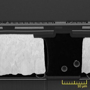
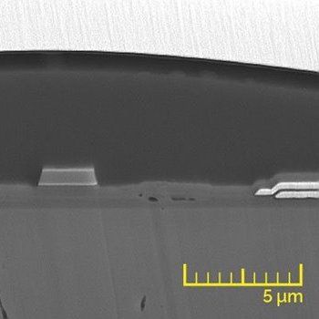
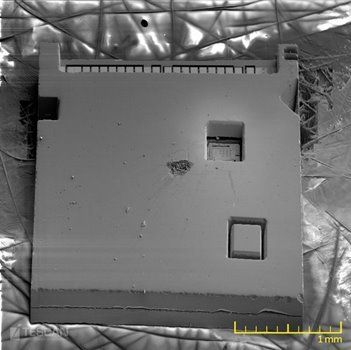
Failure analysis of integrated circuits
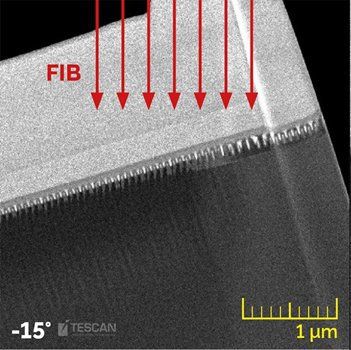
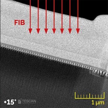
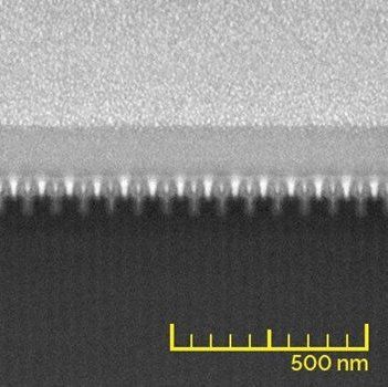
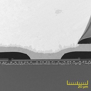
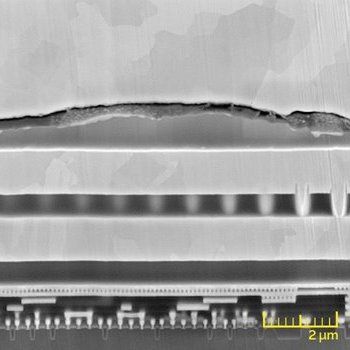
The semiconductor industry continues to shrink the size of electronic devices and sub-20 nm technology nodes are already available.
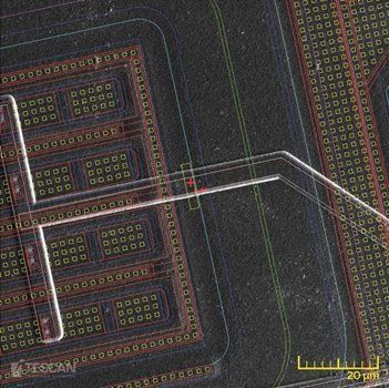
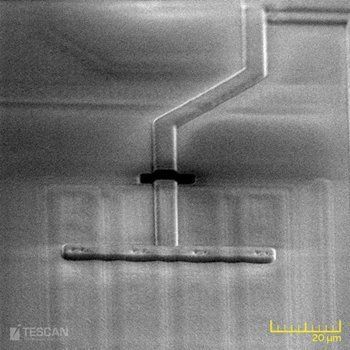
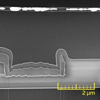
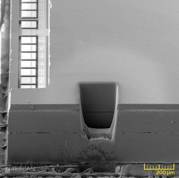
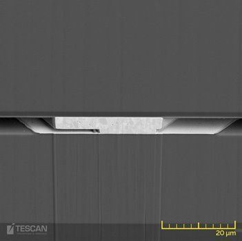
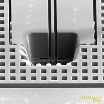
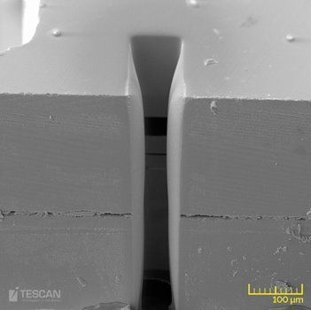
Circuit Edit
Circuit edit (CE) is a common technique used in the design-debug phase of integrated circuits. Most CE activities are performed by means of FIB systems equipped with a Gas Injection System (GIS). Such systems allow site-specific and precise material etching as well as the deposition of conductive contacts or insulation.
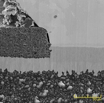
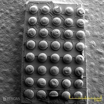
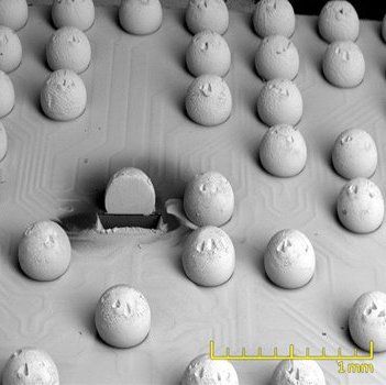
Ball grid Array (BGA)
Ball grid array (BGA) is a surface-mount packaging technology consisting of an array of solder balls on the underside of a chip package. BGA has been developed in response to the trend in the semiconductor industry towards the miniaturisation of ICs, and in pursuit of higher integration, higher density, and improved functionality.
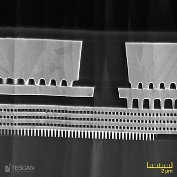
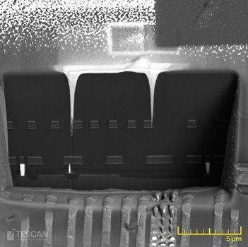
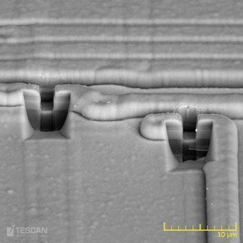
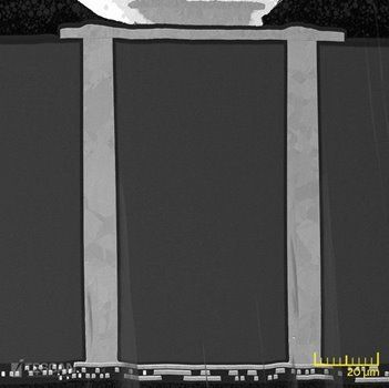
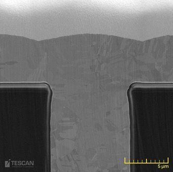
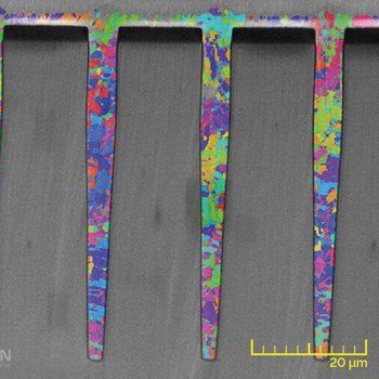
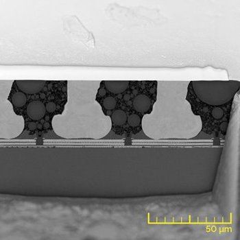
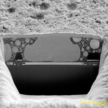
Through Silicon Vias
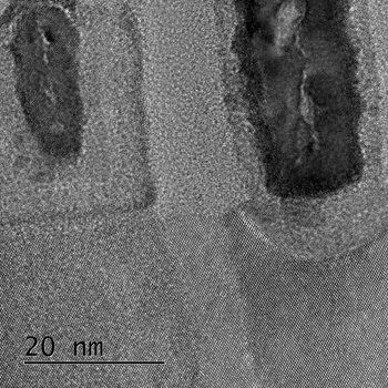
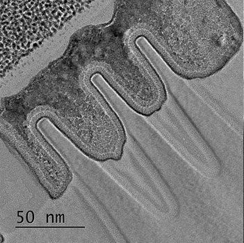
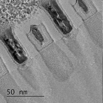
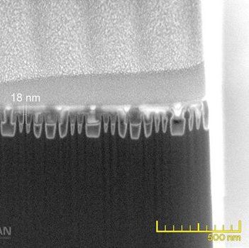
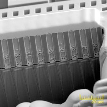
Through-silicon vias (TSVs) is an advanced 3D interconnect technology and a crucial component to make 3D integration packaging possible. TSVs vertically interconnect die stacks which results in improved electrical performance (such as high conductivity and low RC delay), lesser power consumption, and form factor for 3D integrated circuits.
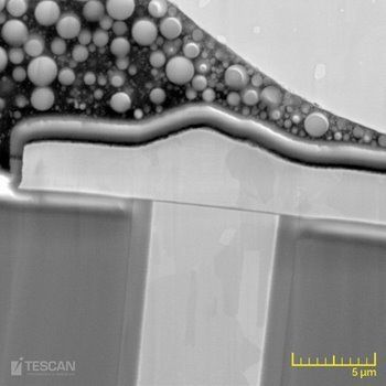
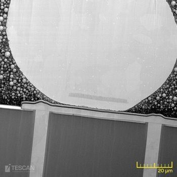
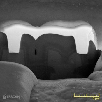
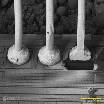
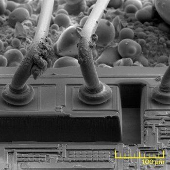
Wire Bonding
Using ultra-fine bonding wires of copper and gold continue to be the most widely used method for creating interconnections in high-density multi-chip modules in the microelectronic and semiconductor industry.
Displays
The development of displays has progressed rapidly in recent years, and this has resulted in high quality displays which deliver sharp and bright images, wide viewing angles, vivid colours, all in a touch-sensitive layer.

Micro-electro-mechanical Systems
Micro-Electro-Mechanical Systems (MEMS) is a technology which can be defined most generally as miniaturised mechanical and electro-mechanical elements which are commonly made of Si substrate and fabricated by means of photolithography and chemical etching.
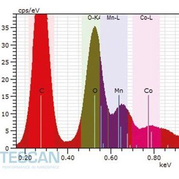
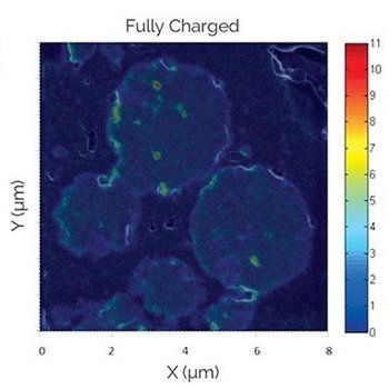
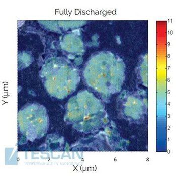
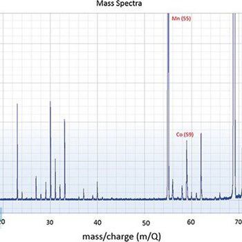
Batteries
There is relentless research in the battery industry which aims at developing the future energy storage systems, a task which continues to be one of the crucial technological challenges. For this purpose, a series of analyses and the characterisation of product reaction effect on electrodes that take place especially at their surface and interface regions are essential. This requires analytical techniques capable of differentiating chemical states with high sensitivity and high spatial resolution.