Material science
Characteristics of materials, such as their structural, mechanical, chemical, electrical, and magnetic properties.

1D materials
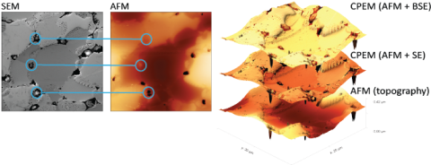
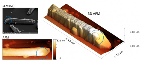
Gallium arsenide (GaAs) nanowires
GaAs nanowires have been explored for a wide variety of potential devices, including transistors, photodetectors, LEDs, solar cells, and nanolaser devices. The optimization of the synthesis of GaAs nanowires is crucial to obtain the expected characterizations. Correlative AFM-in-SEM microscopy facilitates efficient quality control and complex analysis of nanowires.
Benefits of LiteScope:
- Fast and precise localization of a single nanowire. Complex characterization of structures and chemical composition of a single nanowire using SEM material contrast and 3D AFM profiles.
Published courtesy of: David Fuster, Andrés Raya, Álvaro San Paulo and María Ujue González, CNM, CSIC Madrid, Spain
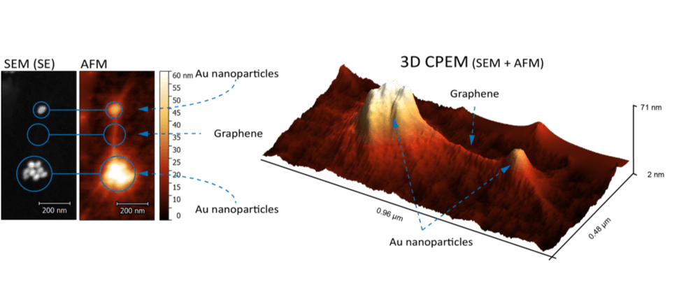
Gold nanoparticles covered by a layer of graphene
Graphene has the potential to create next-generation electronics: faster transistors, semiconductors, and other electronics. Graphene is also used for surface enhanced Raman spectroscopy (SERS), which increases the Raman signal for ultrasensitive analytical applications.
Graphene-veiled gold nanoparticles are candidates for this application. Analysis of such a sample is difficult using separate SEM and AFM techniques. SEM provides contrast only on gold nanoparticles, while AFM can easily visualize the graphene coating, but generally has difficulty imaging small spherical objects.
Benefits of LiteScope:
- Fast and accurate localization of individual nanostructures.CPEM combines the imaging strengths of SEM (imaging of gold nanoparticles) and AFM (imaging of graphene and particle cluster topography).
Published courtesy of: Martin Konecny, CEITEC BUT, Czechia
2D materials
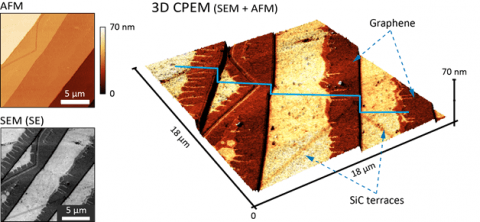
Graphene on silicone carbide (SiC)
Graphene prepared by thermal decomposition of SiC forms mainly at the edges of SiC terraces. Graphene growth is very sensitive to temperature during the etching process and the final quality of the layer can differ from sample to sample. The AFM-in-SEM approach enables fast and efficient quality analysis of the sample.
Benefits of LiteScope:
- Quick identification of the area of interest in the sample. Combination of SEM material contrast with AFM topographic evaluation and monolayer resolution. All in one measurement.
Posted courtesy of: Jan Kunc, MFF UK, Czechia
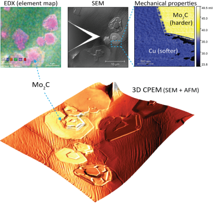
Molybdenum Carbide Mo2C Complex Analysis
Mo2C represents a novel 2D material that can be applied in a multitude of clean energy technologies that are based on the hydrogen evolution reaction (HER). Carbides of different shapes (eg, hexagonal, triangular, rectangular) are highly active and stable for HER; therefore, AFM in SEM is an ideal tool for imaging and complex correlative analyzes (topography, elemental analysis, mechanical properties...) of Mo2C to improve its catalytic properties.
Benefits of LiteScope:
- AFM-in-SEM enables complex correlative imaging and analysisSEM-EDX: Material contrast and elemental analysisAFM: Topography and mechanical properties of materialsCPEM accurately correlates chosen AFM and SEM dataPrecise and fast localization of nanostructures.
Published courtesy of: Prof. Zdeněk Sofer, UCT Prague, Czechia
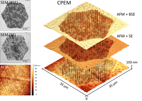
Graphene on Cu foil
In this application, graphene serves as a protective layer on the surface. The copper foil under the graphene is protected against oxidation and its surface structures are preserved, unlike the environment of the graphene flakes.
Benefits of LiteScope:
- The AFM-in-SEM approach enables rapid and accurate localization of a single graphene flake in the sample and its complete characterization: CPEM can accommodate multiple channels from both AFM (eg topography) and SEM (eg ., secondary electrons and backscattered electrons).
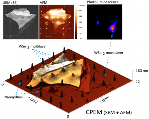
WSe2 flakes on Si nanopiles
The WSe2 monolayer represents a transparent photovoltaic material with LED properties. It is an ideal material for devices with tunable band gaps, which means LEDs can be made from a single material. The determined shape of the monolayer on the nanopillars forms a single photon emitter.
Benefits of LiteScope:
- Precise and fast localization of nanostructures. SEM contrast and AFM topography allow easy interpretation of data with single-layer resolution.
Published courtesy of: Veronika Hegrová, NenoVision, Czechia and Martin Konecny, CEITEC BUT, Czechia
Graphene on platinum
Progress in large-scale, high-quality graphene synthesis is commendable, however, structural controllability and membrane homogeneity are major puzzles facing researchers. CPEM technology, which combines the strengths of AFM and SEM, represents the perfect tool for in situ analysis and optimization of graphene growth.
Benefits of LiteScope:
- Fast and accurate location and characterization of graphene crystals and their small surface nuances. The CPEM view highlights the uneven surface of platinum covered by graphene, as well as the material contrast between the two materials. It quickly answers questions about flake shape and reveals the presence of two graphene crystals bonded close to each other.
Published courtesy: Guido Janssen, TU Delft, The Netherlands
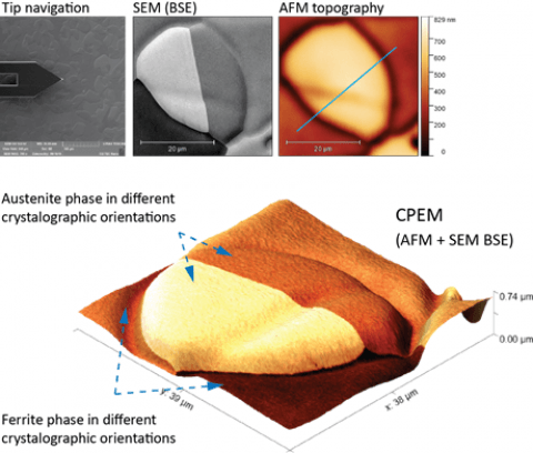
Ferritic-austenitic steel
Duplex stainless steels have a microstructure made up of two main phases: ferrite and austenite. They are used in a wide range of applications due to their advantageous properties.
High temperatures during manufacturing processes can change the balance of alloying elements and cause drastic deterioration in the toughness, corrosion resistance and weldability of duplex stainless steels. Therefore, detailed analysis of the microstructure of duplex steels is essential.
Benefits of LiteScope:
- The AFM-in-SEM approach enables the rapid and accurate localization of a single grain in the sample and its complete characterization, including phase identification, crystallographic orientation, and topographic measurement. All in one measurement.
Posted courtesy of: Marina Knyazeva, TU Dortmund, Germany
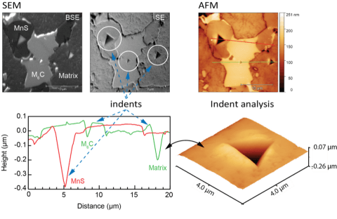
High speed steel nanoindentation M3 class 2
In this case, the AFM-in-SEM approach was further extended by adding a nanoindenter to the LiteScope scanning head. Nanoindentation represents an extremely versatile technique for determining the mechanical properties of materials at the nanoscale, such as modulus of elasticity, hardness values, fracture or creep toughness, and yield strength. This hybrid technique enabled sample phase identification, precise indentation orientation, and topographic analysis, all in a single measurement.
Benefits of LiteScope:
- Fast and accurate identification of a wide range of small-sized separated phases. Indentation of individual phases with nanometer precision. Accurate indentation analysis by AFM.
Published courtesy of: C. Julia-Schmutz, CSEM SA Neuchâtel, Switzerland
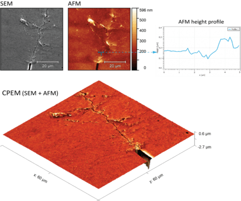
Crack propagation in chrome steel
The fatigue crack propagation behavior of chrome steel was studied using the AFM-in-SEM technique in combination with a focused ion beam (FIB). The crack was initiated using the FIB on the steel sample mounted in a tension/compression module and the crack propagation was analyzed simultaneously by both AFM and SEM.
Benefits of LiteScope:
- Accurate crack initiation and location by SEM-FIB. Analysis of crack propagation after cyclic loading by both techniques. The 3D CPEM view allowed a detailed analysis and better understanding of the data obtained.
Published courtesy of: Ing. Ivo Kuběna, Ph.D.
Decomposition of W-Cr annealed solid solution with HfO2 particles
Tungsten alloys represent promising candidates to replace tungsten in early wall applications in future melting facilities. Since tungsten is susceptible to oxidation at elevated temperatures, various oxide-forming elements (chromium, titanium, silicon) are added to tungsten to induce self-passivation.
In this paper, alloy W-10Cr-1Hf with dispersion of hafnium oxide particles was prepared by plasma spark sintering, in which unique microstructure features were discovered by AFM-in-SEM approach.
Benefits of LiteScope:
- Quick and precise localization of the region of interest. CPEM view. Visualization of differences between contrast of material (SEM) and topography (AFM). CPEM can accommodate multiple channels (eg BSE, SE and topography).
Published courtesy of: Monika Vilemova, Institute of Plasma Physics AS CR, Czech Republic