
LiteScope™ Measurement Modes
Mechanical properties of materials
| Technique | Request |
|---|---|
| Atomic Force Microscopy (AFM) | topography |
| power dissipation | local elastic properties (tapping mode) |
| Force Modulation Microscopy (FMM) | local elastic properties (contact mode) |
| Force-distance curves | local elastic properties (not topographical) |
| Nanoindentation | depth dependent material characterization |
| nanomanipulation | various on-site operations |
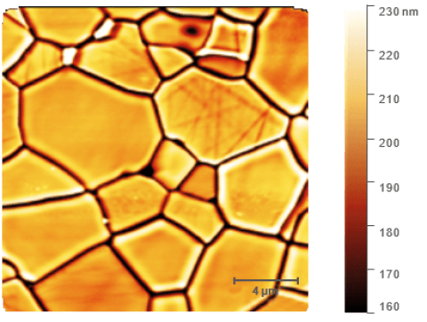
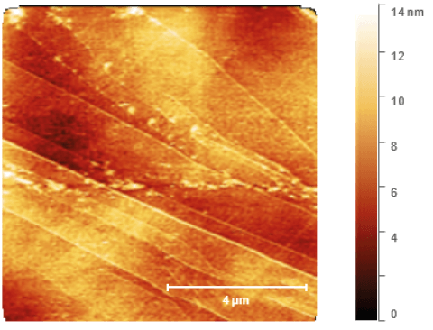
Atomic Force Microscopy (AFM)
AFM enables high-resolution measurements of a wide range of samples.
Different types of self-sensing cantilevers can be used. Measurements can be made in contact or tapping mode.
power dissipation
The energy dissipation provides images of the local elastic properties of the material. Thanks to the use of the AFM tapping mode, the risk of sample damage is minimized compared to FMM. The power dissipation information is read from the amplitude of the drive signal.
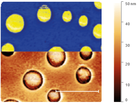
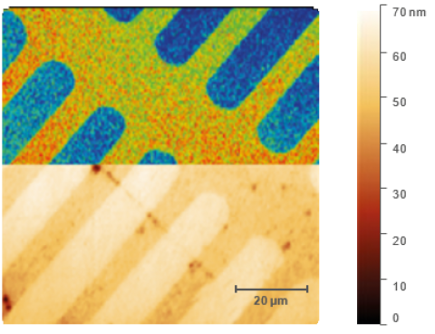
Force Modulation Microscopy (FMM)
FMM allows to obtain images of the local elastic properties of the sample. This method simultaneously measures the topography and the mechanical response of the material to mechanically excited cantilever oscillations. The amplitude and phase of the demodulated signal contain information about the local elasticity.
Nanoindentation
Widely used method for the characterization of the hardness of materials. The hardness of the sample is determined from the depth of the indentation profile and the force used.
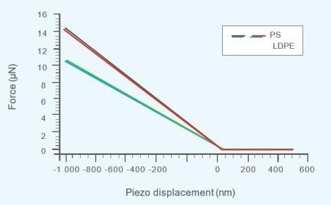
Force-distance curves
F/z spectroscopy is a useful tool for precise characterization of local samples. Spectroscopy is used for many purposes, such as a sample stiffness analysis, detailed surface tip force progress, or determination of local elasticity/plasticity.
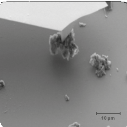
nanomanipulation
Mechanical and electrostatic manipulation enables in-situ movement of the particles with nanometer precision. It can be used instead of or with SEM nanomanipulators for complex in-situ operations.
Electrical properties of materials
| Technique | Request |
|---|---|
| AFM conductivo (C-AFM) | conductivity map |
| CPEM conductivo (C-CPEM) | conductivity map including isolated areas |
| Force Modulation Microscopy (FMM) | local elastic properties (contact mode) |
| Kelvin probe force microscopy (KPFM) | local surface potential |
| electrical spectroscopy | local electrical properties (not topographical) |
| Scanning Tunneling Microscopy (STM) | sub-nanometer topography |
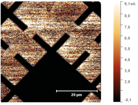
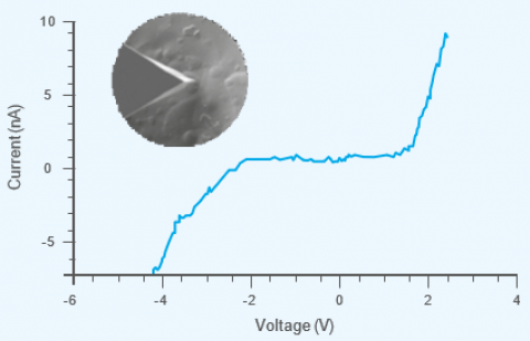
AFM conductivo (C-AFM)
Conductive AFM provides a high resolution local conductivity map of the sample. The voltage bias is applied between the tip and the sample and the current flow between the tip and the sample is measured during the contact AFM topography measurement.
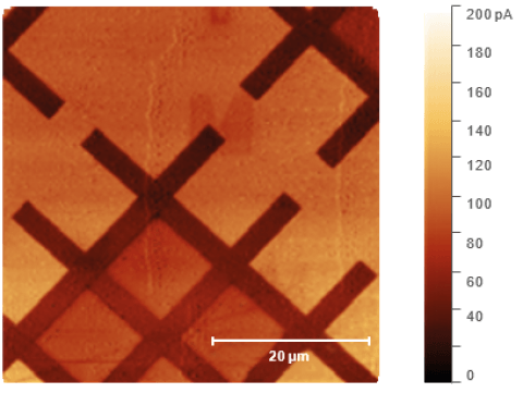
CPEM conductivo (C-CPEM)
The unique conductive CPEM allows conducting conductivity measurements even in isolated areas of the sample. The electron beam at the constant tip distance replaces the need for a polarization applied to the measured area, but the tip sample polarization can still be applied simultaneously. During the scan, the tip-to-sample current flow is measured in contact AFM mode.
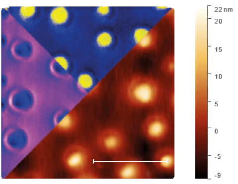
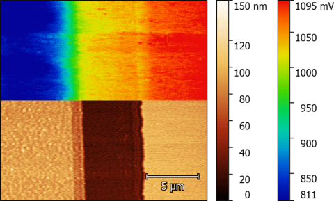
Kelvin probe force microscopy (KPFM)
KPFM estimates the local distribution of surface potentials. First, the topography is measured in the tapping AFM mode. Second, the probe is raised and probe oscillation (AM-KPFM) or resonant frequency change (FM-KPFM) is minimized by applying DC voltage in a feedback loop.
Spectroscopy modes
LiteScope™ provides a wide range of complex spectroscopic techniques. Spectroscopy modes allow measurement of the time dependence of the selected quantity, voltage bias, tip-to-sample distance, electron beam current, etc. The entire process can be monitored by SEM for the exact location of the tip in the sample.
Scanning Tunneling Microscopy (STM)
STM allows the measurement of conductive or semiconducting samples with sub-nanometer resolution. The bias voltage is applied and the tip-to-sample tunneling current is measured. STM provides topographical information about the sample. Measurements are made in constant current or constant height mode.
Electromechanical properties of the material.
| Technique | Request |
|---|---|
| Piezoelectric Response Force Microscopy (PFM) | piezoelectric domain imaging |
Piezoelectric Response Force Microscopy (PFM)
PFM allows imaging and manipulating domains of piezoelectric materials. This method simultaneously measures the topography and the mechanical response of the material to the applied alternating voltage. The amplitude and phase of the demodulated signal contain information about the local piezoresponse.
Magnetic properties of materials
| Technique | Request |
|---|---|
| Magnetic Force Microscopy (MFM) | magnetic domain imaging |
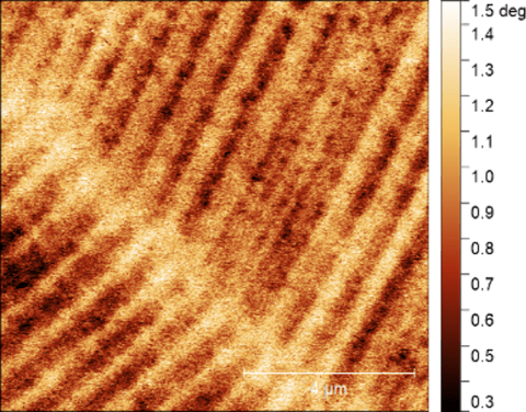
Magnetic Force Microscopy (MFM)
Magnetic force microscopy (MFM) is a secondary imaging mode that maps the magnetic force gradient on the sample surface and at the same time obtains topographical data.
Potential application: magneto-optical recording, magnetic logic and data storage systems.

Birthday Sparks
Fashion Magazine