Applications:
Nanostructures
On-site analysis of special applications such as surface modification, failure analysis and chemical analysis of surfaces
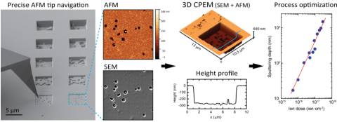
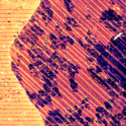
Surface modification of cadmium telluride
Cadmium telluride (CdTe) is a semiconductor with a wide range of applications ranging from X-ray or gamma-ray detectors to solar cells. Due to the heterogeneity of the CdTe compound, the planarity of the focused ion beam (FIB)-etched structures is uneven and requires optimization of the FIB milling process.
Benefits of LiteScope:
- Surface modification using FIB/GIS techniques can be performed directly on a tilted LiteScope within SEM, which is crucial for sensitive samples prone to oxidation.Immediate evaluation of the modified surface profile and process quality control.Process optimization FIB milling by sputtering rate and roughness estimation.
Published courtesy of: Ondrej Sik and Martin Konecny, CEITEC BUT, Czech Republic, and Veronika Hegrová, NenoVision, Czech Republic.
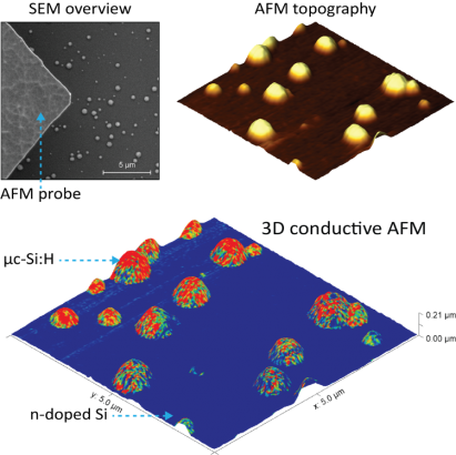
Conductivity mapping of microcrystalline silicon
Microcrystalline silicon is a silicon film where the sizes of the silicon crystals are in the order of tens of nanometers. μc-Si:H thin films are suitable for various devices, such as TFT, thin solar cells with higher IR absorption and more stable against solar radiation. LiteScope supports conductive AFM ( cAFM ) analysis within SEM, helping to easily locate particular structures and assess conductivity mapping with nanometer accuracy.
Benefits of LiteScope:
- AFM-in-SEM enables complex correlative imaging and analysisSEM: contrast materials and rapid localization of nanostructuresc-AFM: topography and conductivity mapping
Posted courtesy of: RNDr. Antonín Fejfar, Czech Academy of Sciences, Czechia
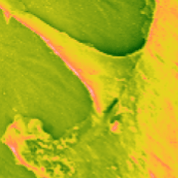
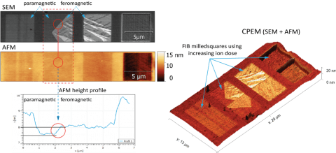
Fe78Ni22 Magnetic Nanopatterns Using a Focused Ion Beam
The metastable Fe78Ni22 thin film growing on a copper substrate has the potential to form magnetic patterns: it is paramagnetic at room temperature, but can be transformed by FIB irradiation into a ferromagnetic material. Simultaneous measurement of AFM and SEM signals revealed that the crystallography transformation is accompanied by a topography change.
Benefits of LiteScope:
- Surface modification using FIB/GIS techniques can be performed directly on a tilted LiteScope within SEM, which is crucial for sensitive samples prone to oxidation. Immediate evaluation of the modified surface profile and process quality control.
Published courtesy of: Lukas Flajsman, CEITEC BUT, Czechia
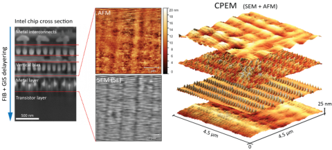
Integrated Circuit Pickling
Due to miniaturization, failure analysis of advanced integrated circuits is only possible by removing locally focused ion beam (FIB) layers. It is necessary to analyze the flatness and roughness of the pickled surfaces.
Benefits of LiteScope:
- Precise identification of a particular layer, excellent planarity of milled FIB structures with minimal damage to the sample. 3D Reconstruction: in situ evaluation of the topography and roughness of the milled structure.
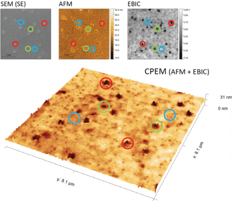
Images of thread dislocations in GaN/AlN/Si films
Gallium nitride (GaN) is a very promising material for electronic and optoelectronic applications; however, a variety of dislocations can occur at the interface of different materials, leading to poor quality films.
Benefits of LiteScope:
- Various defects can be located and characterized only by the CPEM view, which combines AFM, SEM, and EBIC (Electron Beam Current) CPEM allows direct comparison between surface topography, electrical activity, and surface chemistry of the sample.
Published courtesy of: Roman Gröger, IPM CAS, Czech Republic
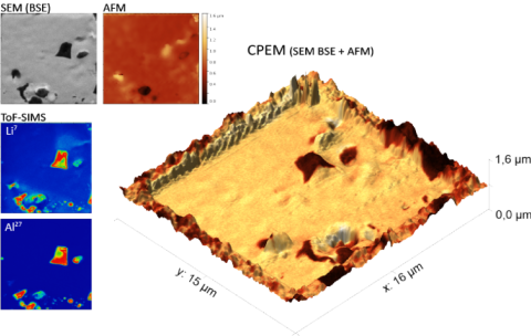
Correlative images combining AFM-in-SEM and ToF-SIMS of metal with Li and Al particles
Secondary ion time-of-flight mass spectrometry (ToF-SIMS) provides elemental, chemical and molecular state information on the surfaces of solid materials. The alloy with lithium and aluminum particles is used to verify the sensitivity of SIMS detectors for light elements.
The correlation of SEM ToF-SIMS with AFM provides the missing sample topography and allows the calculation of, for example, sputtering rates to optimize the process, which is crucial especially for heterogeneous materials.
Benefits of LiteScope:
- Fast and precise localization of surface structures. Initial evaluation of the topography of the sample and 3D CPEM visualization of the sprayed volume containing the contrast of the SEM material.
Material science
More information
semiconductors